Ever wondered how your smartphone or computer actually works? It all starts with something called PCB assembly — the process that brings electronic circuits to life. Without it, modern devices wouldn't exist.
PCB assembly connects all the essential components onto a circuit board. Understanding this process helps you design better, fix issues faster, and avoid costly mistakes.
In this post, you'll learn what PCB assembly is, why it's important, and how each step works — from start to finish.
What Is PCB Assembly?
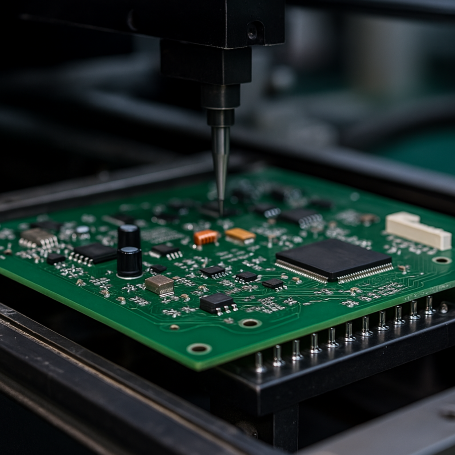
Printed Circuit Boards, or PCBs, are everywhere. From phones to refrigerators, they're the thin, often green boards with copper lines that link different electronic parts. But by themselves, PCBs don't do anything. They're just the empty roads. What makes them work is the process of PCB assembly, or PCBA.
Here's where it gets interesting. A PCB is just the base—like a blank canvas. PCBA means we're actually adding the components, like resistors, chips, and connectors, onto that board so it can function. This is done using different technologies, often SMT and THT, and includes soldering, inspection, and testing.
It's easy to confuse PCB manufacturing with assembly, but they're not the same. Manufacturing focuses on making the bare board using layers of copper, fiberglass, solder mask, and silkscreen. Assembly happens after that—it's all about placing and securing the parts that make the board work.
You'll find assembled PCBs in all sorts of electronics. Think smartphones, TVs, electric bikes, washing machines, routers, or even machines in factories. Some are tiny, packed with small chips. Others are big and loaded with power-handling parts. No matter the size, PCBA is what turns a quiet board into something that processes, connects, or powers up your device.
Overview of the PCB Assembly Process
Before a circuit board does anything useful, it goes through several key stages. The PCB assembly process is a mix of automated steps and hands-on work. It all starts with pre-assembly, moves through SMT and THT stages, and ends in post-processing.
During pre-assembly, the focus is on reviewing the design. This means checking the Gerber files and BOM, or Bill of Materials. These files tell the assembler what to build, what parts are needed, and how they fit together. A solid BOM avoids delays, missing parts, or errors later. Engineers also run DFM checks to make sure the board is actually buildable. If spacing is off or pads are too small, problems pop up fast.
Next comes the SMT stage. This is where tiny components are placed on the surface of the board. Machines apply solder paste to specific spots, then pick and place components with robotic precision. After that, the board goes into a reflow oven so the paste melts and hardens into solid joints.
If there are larger parts that can't be mounted on the surface, we move to THT. Here, parts with long leads go through holes in the board. These are soldered either by hand or by wave soldering, where molten solder flows across the bottom of the board.
After assembly, it's time for post-processing. That includes cleaning the board, programming any chips, running functional tests, and sometimes adding a protective coating. These steps make sure the board not only works, but stays reliable when used in the real world.
Major Steps of the PCB Assembly
Stage 1: Pre-Assembly Preparation
Before any components touch the board, the pre-assembly phase sets the tone for everything that follows. At this point, design files are double-checked, parts are sourced, and the groundwork is laid to avoid problems down the line.
What Is DFM/DFA Analysis?
DFM stands for Design for Manufacturability. It's a process where engineers review your circuit layout and component placements to spot anything tricky or risky to build. Maybe two pads are too close. Maybe the traces can't handle the current. DFM helps catch those issues early.
DFA, or Design for Assembly, looks at how easy it is to actually put everything together. Even if the design functions on paper, will it work during high-speed assembly? Could something shift during reflow or get blocked during inspection? That's what DFA helps answer.
Both DFM and DFA prevent costly rework, delays, and defects. They save time and materials by making sure the board design won't cause problems during production.
Component Procurement and Quality Control
Once the design passes inspection, it's time to gather parts. The Bill of Materials, or BOM, lists every resistor, capacitor, chip, and connector the assembly will need. But ordering them isn't just clicking a button.
Manufacturers need to find trusted suppliers that offer original, tested components. No knock-offs. Once the parts arrive, incoming quality control kicks in. This step verifies the size, packaging, and condition of every batch. Parts with bent leads or broken reels don't go on the board.
Having verified components in hand means the SMT and THT stages can begin smoothly—without risking reliability or compliance.
Stage 2: Surface Mount Technology (SMT) Assembly
Surface mount technology, or SMT, handles the tiny components that sit flat on the board. These include most resistors, diodes, and integrated circuits. It's the most efficient and widely used method for modern electronic assembly.
What Is SMT in PCB Assembly?
SMT allows machines to quickly place parts with incredible accuracy. Unlike the older through-hole method, which needs leads pushed through holes, SMT places parts directly onto the board surface. It's fast, compact, and great for high-density layouts.
Step 1: Solder Paste Application
Every component needs a sticky landing spot. That's where solder paste comes in. This paste is a mix of powdered metal—mostly tin—with a bit of silver and copper. Flux is added to help it melt and flow later.
A metal stencil is placed over the bare PCB, and the paste is carefully printed onto the pads. Machines spread the paste evenly using a blade. Once the stencil is removed, the board holds small blobs of paste only where needed.
Too much paste? It could short two pads. Too little? A weak joint or no connection. That's why this step is critical.
Step 2: Pick-and-Place of SMD Components
Now that the board is prepped, robotic arms go to work. Using vacuum nozzles, the pick-and-place machine grabs each part from a reel and places it on the board. Every move is pre-programmed based on the design file. The machine knows exactly where each part belongs.
Small parts like 01005 resistors, which are barely bigger than a grain of dust, are no problem. Larger chips or connectors are also placed, just with different nozzles.
This process can happen at lightning speed—placing thousands of components per hour—without mistakes or fatigue.
Step 3: Reflow Soldering Process
Now the parts need to be secured. That's the job of the reflow oven. The entire board travels on a conveyor belt through a long chamber that heats in stages.
At first, the temperature rises gradually to warm the board. Then it peaks above 217°C to melt the solder. Finally, it cools down slowly so the solder solidifies without cracking.
The result? Each component is locked in place by a clean, shiny solder joint. On double-sided boards, one side is done first, then the process repeats for the other side. Careful planning prevents parts from falling off during the second pass.
Step 4: Optical Inspection (AOI)
After reflow, it's time to check for issues. Components might shift slightly or fail to solder. That's where inspection comes in.
Small batches may get a manual look under magnifiers. For higher volumes, automatic optical inspection—or AOI—takes over. These machines scan the board with high-speed cameras. They recognize reflections from the solder to spot cold joints or misaligned parts.
For hidden joints under chips like BGAs, X-ray inspection is used. It lets technicians see through the board to catch defects you can't spot from the surface.
Stage 3: Through-Hole Technology (THT) Assembly
Not all components are surface-mounted. Some still need to go through the board. This is where through-hole technology comes in. Power components, connectors, or transformers often use this method.
What Is THT in PCB Assembly?
THT involves components with long leads that pass through holes in the PCB. These leads are soldered on the other side to create a strong mechanical and electrical connection. It's great for high-stress parts that might face vibration or heat.
Manual Insertion of Through-Hole Components
Most THT starts with a technician placing parts by hand. It's not as fast as SMT, but it offers flexibility. The assembler follows the placement guide, watching for orientation, polarity, and spacing.
Anti-static precautions are a must, especially for sensitive chips. One wrong zap can ruin an expensive component.
Once placed, the board is moved to the soldering area.
Wave Soldering Explained
For larger batches, wave soldering is the go-to method. Boards travel over a bath of molten solder. A wave rises up and touches the underside, soldering all exposed leads in seconds.
This method is fast and reliable—but it's only for single-sided or selective assemblies. Double-sided boards need special handling or manual soldering to avoid damaging parts already in place.
Stage 4: Post-Assembly Procedures
Once all the parts are on and soldered, there's still more to do. Post-processing ensures the board is clean, functional, and protected.
Cleaning and Flux Removal
Soldering leaves behind flux. It looks harmless but can corrode joints over time. It also traps moisture and dust. That's why cleaning is essential.
Technicians use deionized water and high-pressure washers. No ions means no short circuits. Afterward, compressed air removes moisture to leave the board dry and ready.
Final Inspection and Touch-Ups
Before anything ships, there's one more inspection. Technicians look for solder bridges, missing parts, or cosmetic defects. X-ray is used again if needed.
If any problems are found, they're fixed manually. A soldering iron and some flux can repair cold joints or fill in weak areas.
IC Programming
Some boards need a brain. That's where firmware comes in. Using a USB interface, the software is uploaded to the IC on the board.
This step can include calibration or version checks, depending on the project. Without programming, the board may look perfect but do nothing.
Functional Testing (FCT)
The last big test simulates real-world use. Power is applied. Signals are sent. Technicians watch how the board responds. Is the voltage steady? Does the screen light up? Do buttons work?
If anything is off, it's noted and fixed. This is the final step before boards go into products—or fail and get scrapped.
PCB assembly may sound simple at first, but every step is packed with detail and precision. Each part, joint, and trace plays a role in making electronics work the way we expect them to.
SMT vs THT vs Mixed Technology in PCB Assembly
When assembling PCBs, there's no one-size-fits-all method. Surface Mount Technology (SMT), Through-Hole Technology (THT), and Mixed Technology each have their own strengths and limits depending on the project.
SMT is fast, compact, and highly automated. It's perfect for small parts like resistors or ICs, especially when you're producing large batches. Machines handle almost everything, which keeps labor costs low. But it doesn't work well for big, heavy components that need mechanical strength.
That's where THT comes in. It's great for connectors, coils, or power parts that need to stay firmly attached. Components go through the board and are soldered on the other side. It takes longer and costs more, especially when done manually, but offers stronger physical support.
Mixed technology uses both. That's common in modern designs where boards carry small logic chips and large power parts. If planned right, both methods work together. Place SMT parts first using reflow, then add THT parts and run wave soldering—or use hand soldering if the quantity is small.
To avoid problems, designers should separate parts by side, avoid tight spacing near holes, and follow the right assembly sequence. Doing this keeps the build smooth and reduces costly rework.
Common PCB Assembly Defects and How to Avoid Them
Even the most advanced assembly lines can run into trouble. Knowing the most common PCB assembly defects helps catch issues early and avoid wasted boards. Here are a few that show up often.
Cold solder joints
This happens when the solder doesn't fully melt or bond. It looks dull or grainy and causes weak or unreliable electrical connections. It usually comes from poor heating during reflow or wave soldering. To avoid it, check temperature profiles and ensure the oven is properly calibrated.
Tombstoning
Tombstoning gets its name from how small parts like resistors stand up on one end, like a headstone. One side of the component lifts off the pad due to uneven heating or too much surface tension from the solder. It's common on tiny chips when paste is applied unevenly. Good stencil design and reflow control help prevent it.
Solder bridging
When solder connects two pads that shouldn't touch, it creates a bridge. This can cause short circuits. Too much solder paste or poor alignment during placement are common causes. Using AOI machines and adjusting stencil thickness can reduce this risk.
Misaligned components
If a component shifts during placement or reflow, it may not connect at all. Machines must be well-calibrated, and paste should be applied evenly to hold parts in place until soldering locks them down.
Conclusion
The process of PCB assembly involves multiple steps, from design checks and component placement to soldering and final testing. Each stage—whether SMT, THT, or a mix—requires attention to detail and precision. Choosing the right method, inspecting often, and ensuring clean assembly help prevent costly issues. For complex projects, it's always smart to work with professionals who understand both the technology and quality standards that ensure every PCB works as expected. Welcome to check out our company's supporting products, such as PCB Grinding Brushing Machine, UV Drying Equipment.
FAQs
What is the difference between PCB and PCBA?
PCB refers to the bare printed circuit board without any components. PCBA means the board has all components assembled and is ready for use.
Why are both SMT and THT used in PCB assembly?
SMT is great for small, lightweight components. THT is better for parts that need strong mechanical support. Many boards use both methods.
What is the purpose of reflow soldering?
Reflow soldering melts solder paste so it bonds components to the board. It's key to securing surface-mounted devices.
How do you prevent soldering defects like bridging?
Use the right stencil thickness, apply paste carefully, and run regular inspections like AOI to catch problems early.
Can one PCB have components on both sides?
Yes, double-sided boards are common. Each side is assembled and soldered separately, often starting with the simpler side.


