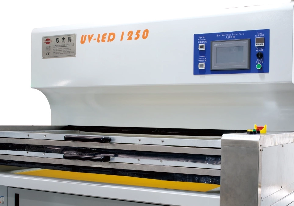
The printed circuit board (PCB) industry is the backbone of modern electronics, enabling the production of intricate electronic devices with high precision and efficiency. One of the most critical steps in PCB manufacturing is the exposure process, where patterns are transferred from a photomask onto a substrate using a light-sensitive material. This process is facilitated by a PCB exposure machine, a specialized tool that ensures high-resolution patterning and alignment.
Understanding the PCB exposure process is vital for achieving optimal performance and reliability in electronic devices. This article will explore the role of PCB exposure units, the principles of photoresist chemistry, the general steps in the exposure process, key techniques, and factors influencing quality. Additionally, we will discuss the consequences of poor exposure and its impact on production efficiency.
What Is Photoresist in PCB Production?
Photoresist is a light-sensitive material applied to the surface of a PCB during the exposure process. It serves as a medium for transferring the intricate patterns required for circuit formation. Photoresists are typically classified into two types: positive and negative, each reacting differently when exposed to light.
A PCB exposure unit uses ultraviolet (UV) light to alter the chemical properties of the photoresist, enabling selective development. The choice of photoresist depends on the desired resolution, manufacturing requirements, and the specific application of the PCB.
Types of Photoresist
Positive Photoresist: Becomes soluble in the exposed regions, allowing those areas to be removed during development.
Negative Photoresist: Hardens in the exposed regions, leaving those areas intact after development.
Photoresists are critical in ensuring high precision during the exposure process, directly influencing the resolution and accuracy of the final PCB.
Chemical Changes When Photoresist Exposed to Light
The exposure process relies on the chemical transformation of photoresist materials under light. This transformation is what enables the selective removal or retention of specific areas during subsequent processing steps.
Chemical Principle of Positive Photoresist
Positive photoresist contains a light-sensitive compound known as a diazonaphthoquinone (DNQ). When exposed to UV light from a PCB exposure machine, DNQ undergoes a photochemical reaction, producing a carboxylic acid. This reaction increases the solubility of the exposed regions in a developer solution. The result is the removal of exposed areas, leaving the unexposed regions intact.
Chemical Principle of Negative Photoresist
Negative photoresist behaves differently. It contains photo-initiators and polymers that crosslink when exposed to UV light. The exposure causes the exposed areas to harden and become insoluble in the developer solution. In this case, the unexposed regions are removed, leaving the hardened pattern behind. Negative photoresists are often used for applications requiring higher durability.
General Steps of the Exposure in PCB Production
The exposure process in PCB manufacturing involves several systematic steps, which are as follows:
Photoresist Application: The substrate is cleaned and coated with a uniform layer of photoresist.
Alignment with Photomask: A photomask containing the circuit pattern is aligned with the substrate.
Exposure: The substrate is exposed to UV light using a PCB exposure unit.
Development: The exposed substrate is treated with a developer solution to remove selected areas of the photoresist.
Etching: After development, the substrate undergoes etching to remove unprotected areas, forming the desired circuit pattern.
Final Cleaning: Residual photoresist is removed, leaving behind the completed circuit.
Each step requires precision and control to ensure high-quality results.
Main Exposure Techniques
The PCB exposure machine plays a crucial role in determining the quality and resolution of the pattern transfer. Different exposure techniques are used based on the production requirements, each with its strengths and limitations.
Contact Printing
In contact printing, the photomask is placed in direct contact with the photoresist-coated substrate. UV light passes through the mask, exposing the photoresist. While this method offers high resolution, it may cause wear on the photomask over time, making it less suitable for mass production.
Proximity Printing
Proximity printing involves a small gap between the photomask and the substrate. This method reduces wear on the mask but sacrifices some resolution. It is often used for applications where slight compromises in precision are acceptable.
Projection Printing
Projection printing uses an optical system to project the photomask pattern onto the substrate. This method allows for high resolution and is widely used in advanced PCB production. The equipment is more complex and expensive than other techniques, but it offers excellent results for fine details.
Direct Imaging (DI)
Direct imaging eliminates the need for photomasks altogether. Instead, a laser or digital light source directly exposes the photoresist, creating the desired pattern. This technique is highly flexible and well-suited for prototypes and small-scale production. DI is becoming increasingly popular due to its adaptability and reduced material costs.
Factors Affecting the Quality of Exposure
Several factors influence the success of the PCB exposure process. These factors must be carefully controlled to ensure high-quality results.
Alignment Accuracy
Precise alignment between the photomask and the substrate is critical to achieving accurate pattern transfer. Misalignment can result in defective circuits or poor layer registration.
Light Source Quality
The quality of the UV light source in a PCB exposure unit significantly affects resolution. Uniform intensity and wavelength stability are essential for consistent exposure.
Photoresist Quality
The type, thickness, and uniformity of the photoresist layer directly influence resolution and pattern fidelity.
Exposure Time
Correct exposure time is crucial. Overexposure or underexposure can lead to incomplete pattern transfer or other defects.
Environmental Conditions
Temperature, humidity, and cleanliness of the production environment can impact the photoresist's performance and overall exposure quality.
Photomask Quality
Defects in the photomask can lead to errors in the transferred pattern. High-quality photomasks are essential for precise exposure.
Substrate Quality
The smoothness and cleanliness of the substrate surface affect photoresist adhesion and pattern accuracy.
Equipment Calibration
Regular calibration of the PCB exposure machine ensures consistent performance and minimizes defects caused by equipment errors.
The Role of Exposure in PCB Manufacturing
The exposure process is fundamental to high-quality PCB production. It ensures the accurate transfer of patterns and facilitates subsequent processing steps.
Pattern Transfer
The exposure process enables the precise transfer of intricate circuit patterns onto the substrate, forming the foundation of the PCB.
Selective Development
Selective exposure and development allow for the creation of complex circuit designs with high precision.
High Resolution and Fine Detail
Modern PCB exposure machines are capable of achieving resolutions as fine as a few microns, enabling the production of advanced PCBs for cutting-edge technologies.
Layer Alignment
Proper exposure ensures accurate alignment between layers in multi-layer PCBs, which is critical for functionality.
Process Efficiency
Efficient exposure machines and techniques reduce production time, costs, and material waste, enhancing overall manufacturing efficiency.
Consequences of Poor Quality Exposure
Poor exposure quality can lead to various issues, including:
Defective Circuits: Misaligned or incomplete patterns may render the PCB non-functional.
Low Yield: Increased defects result in lower production yields and higher costs.
Reduced Durability: Poor resolution and pattern fidelity can compromise the reliability of the PCB.
Delays in Production: Rework and troubleshooting add to production time and expenses.
Ensuring high-quality exposure is essential to avoid these consequences and maintain product reliability.
Conclusion
The exposure process is a cornerstone of PCB manufacturing, enabling the precise transfer of circuit patterns and ensuring the functionality of electronic devices. The use of advanced PCB exposure machines and a thorough understanding of photoresist chemistry are critical to achieving high-quality results. By carefully controlling factors such as alignment, light source quality, and exposure time, manufacturers can produce reliable PCBs with fine details and high resolution.
Advances in exposure techniques, such as Direct Imaging (DI), are transforming the industry, offering greater flexibility and efficiency. However, attention to detail and adherence to best practices remain essential for success in PCB production.
FAQs
1. What is a PCB exposure machine?
A PCB exposure machine is a specialized device used to transfer circuit patterns onto a substrate by exposing photoresist to UV light.
2. What are the main types of photoresist?
The two main types of photoresist are positive and negative. Positive photoresist becomes soluble when exposed to light, while negative photoresist hardens.
3. What is the role of photoresist in the PCB exposure process?
Photoresist serves as a light-sensitive material that enables selective patterning during the exposure process.
4. How does Direct Imaging differ from traditional exposure techniques?
Direct Imaging uses lasers or digital light to expose photoresist directly, eliminating the need for photomasks and offering greater flexibility.
5. What factors affect exposure quality?
Key factors include alignment accuracy, light source quality, photoresist properties, exposure time, environmental conditions, and equipment calibration.


