PCB milling is a subtractive manufacturing technique used in PCB production where a mechanical tool precisely removes unwanted copper from a copper-clad substrate to form the required circuit patterns. Unlike traditional chemical etching, which uses hazardous chemicals to dissolve excess copper, milling relies on physical cutting, offering a cleaner and more environmentally friendly approach.
This process is especially valuable in rapid prototyping and small-batch PCB production, enabling designers and engineers to quickly fabricate functional circuit boards directly from digital designs. Because it does not require masks or chemical baths, PCB milling allows for faster turnaround times and greater flexibility, making it ideal for testing new designs, iterating prototypes, or producing limited quantities without incurring the setup costs associated with mass manufacturing.
Although PCB milling is just one part of the comprehensive PCB production ecosystem, it complements other methods like photolithography and etching by providing an efficient way to bridge the gap between design and full-scale fabrication. Its role in accelerating development cycles and reducing environmental impact highlights its growing importance in modern electronics manufacturing.
Preparing the Design Files
Before milling begins, accurate preparation of design files is crucial to ensure a smooth PCB production process.
1. Creating or Importing PCB Designs
Designs are created or imported using CAD/CAM software like KiCAD, Eagle, or Altium Designer. These tools define traces, pads, holes, and board outlines. Existing Gerber files can also be converted for milling.
2. Generating Toolpaths and G-code
The PCB layout is processed to generate toolpaths for milling traces, outlines, and holes. These are exported as G-code, which controls the milling machine’s movements and settings such as depth, speed, and tool size.
3. Design Verification
Before machining, the design is checked for manufacturability—ensuring trace spacing, drill sizes, and toolpaths are suitable for milling. Simulations or previews help catch errors early and reduce waste in PCB production.

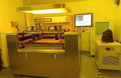
Setting Up the Milling Machine
Proper setup of the milling machine is essential for achieving accuracy and consistency in the PCB production process. This step ensures the equipment is ready to follow the generated G-code instructions precisely.
1. Selecting Appropriate Milling Tools
The choice of cutting tools plays a crucial role in determining the quality of the milled PCB.
End mills are used to isolate copper traces by carving around them.
Drill bits are selected for creating vias and mounting holes.
Tool diameter should match the design requirements, with smaller tools used for fine detail and tighter spacing.
2. Securing the Copper-Clad Board
The copper-clad board must be firmly fixed onto the milling platform using clamps, vacuum tables, or double-sided adhesive. Stability during operation is essential to avoid movement that can cause misalignment or uneven cuts, leading to faulty boards.
3. Calibrating Machine Settings
Once the board is secured and tools are loaded, the machine must be calibrated:
Spindle speed affects cutting efficiency and edge smoothness.
Cutting depth must be carefully set to remove copper without damaging the substrate.
Feed rate controls how fast the tool moves across the surface, balancing speed and precision.
Proper calibration ensures the milling machine performs accurately, resulting in clean, functional boards and minimizing errors in PCB production.
Milling Process Steps
Once the machine is properly set up, the actual milling operations begin. These steps shape the PCB, form the circuit paths, and prepare the board for component assembly — all essential actions in a successful PCB production workflow.
1. Initial Outline Milling
The process often starts with outline milling, where the machine cuts the outer dimensions of the PCB to the specified shape. This defines the board's edges and can include slots or cutouts for connectors, mounting points, or special design features.
2. Isolation Milling
In this step, the tool removes copper from around the traces and pads to electrically isolate them from each other. Known as isolation milling, this is the core task of turning a copper-clad board into a functional circuit. The precision of this operation directly affects signal integrity and the reliability of the final board.
3. Drilling Holes
If the design includes through-hole components or vias, the machine will then drill holes at defined positions. Proper hole placement is critical for electrical connectivity between layers (if applicable) and for accurate component mounting.
4. Final Cleaning and Inspection
After all milling and drilling are complete, the PCB undergoes cleaning to remove debris and copper dust that could cause shorts or interfere with soldering. A visual inspection or continuity test may follow to ensure the board meets design requirements.
Post-Milling Procedures
After the physical milling is complete, several critical post-processing steps are required to ensure the PCB is clean, functional, and ready for assembly. These finishing tasks are essential to the overall quality of PCB production, particularly in prototyping and small-batch fabrication.
1. Removing Residual Dust and Debris
Milling generates fine copper dust and fiberglass particles that can accumulate on the PCB surface and in drilled holes. These residues must be thoroughly removed using compressed air, soft brushes, or ultrasonic cleaning. Clean surfaces prevent contamination, reduce the risk of short circuits, and ensure good solder adhesion during later assembly steps.
2. Electrical Continuity and Short Testing
Once the board is cleaned, it must be tested for electrical continuity and to ensure that there are no shorts between adjacent traces. This can be done manually using a multimeter or through automated test fixtures. Identifying and correcting any issues at this stage prevents failures in downstream stages of PCB production.
3. Preparing for Soldering or Assembly
The final step is preparing the board for component placement. This may include applying flux, verifying pad cleanliness, and checking alignment with the bill of materials (BOM). At this point, the milled PCB is ready for soldering and integration into electronic systems.
Advantages and Limitations of PCB Milling
PCB milling is a practical technique within the broader scope of PCB production, particularly favored in development and low-volume environments. While it offers several key advantages, it also comes with certain trade-offs that must be considered depending on the application.
1.Advantages of PCB Milling
Fast Turnaround Time
PCB milling allows for the rapid fabrication of circuit boards directly from digital designs, eliminating the delays associated with outsourcing or chemical processing. Engineers can go from design to a functional prototype in just hours, making it ideal for quick iterations.
No Use of Chemicals
Unlike traditional etching, PCB milling does not rely on acids or hazardous chemicals. This makes it an environmentally friendly and safer alternative for labs, educational institutions, and workplaces without specialized waste management capabilities.
Ideal for Prototyping and Customization
Because it avoids the overhead of mask preparation or large-scale setup, milling is well-suited for low-volume PCB production, one-off prototypes, and customized designs. It’s also flexible—design changes can be implemented and milled almost immediately.
Conclusion
PCB milling is a valuable and flexible method within the broader landscape of PCB production. From design preparation and machine setup to precise milling and post-processing, each step contributes to creating functional prototypes and small-batch boards efficiently.
While not ideal for large-scale manufacturing, milling excels in speed, adaptability, and chemical-free operation, making it perfect for rapid prototyping and development.
To maximize efficiency and output quality, engineers and manufacturers are encouraged to integrate PCB milling with other PCB production techniques, leveraging its strengths as part of a hybrid manufacturing strategy.


