In today's fast-paced world of electronics manufacturing, precision and efficiency are paramount. As the demand for smaller, more complex, and high-performance electronic devices continues to rise, the need for advanced technologies in PCB (Printed Circuit Board) fabrication is more critical than ever. One such innovation that has significantly transformed the PCB production process is the CCD Line Exposure Machine.
CCD Line Exposure Machines have become an indispensable tool for PCB manufacturers due to their ability to offer highly accurate, consistent, and automated circuit pattern transfers. This technology plays a crucial role in ensuring that the patterns for electronic circuits are transferred onto PCB substrates with minimal defects. However, to fully leverage the benefits of this technology, manufacturers must adopt best practices and tips for optimizing the use of CCD Line Exposure Machines. This article will explore the various ways in which these machines can be optimized for maximum efficiency and quality in PCB production.
1. Understanding the Role of CCD Line Exposure Machines in PCB Production
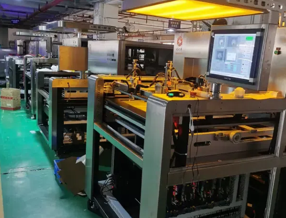
Before diving into the best practices, it's essential to first understand the role that CCD Line Exposure Machines play in PCB production. These machines use Charge-Coupled Devices (CCDs) to align and expose the photosensitive layers on PCBs to ultraviolet (UV) light. This exposure process is vital for transferring the intricate circuit patterns onto the PCB, which will eventually be etched into the board to form the desired electronic circuits.
Unlike traditional exposure methods, CCD Line Exposure Machines offer superior precision and alignment, reducing the risk of defects such as misalignment or distortion. They are particularly valuable in situations where high-density boards with fine traces are required. The ability of these machines to offer automated, highly accurate exposure makes them a popular choice for manufacturers seeking to produce high-quality PCBs at scale.
2. Best Practices for Optimizing CCD Line Exposure Machines
While CCD Line Exposure Machines are powerful tools, their full potential can only be realized when used with the proper practices. Below are several best practices that can help PCB manufacturers optimize the performance of their exposure machines:
A. Regular Calibration and Maintenance
Regular calibration and maintenance are essential to keep your CCD Line Exposure Machine in top working condition. Over time, the machine's alignment can shift, leading to errors in exposure and misalignment of circuit patterns. To maintain high-quality production, you should:
Calibrate the machine regularly to ensure that the CCD alignment is accurate.
Clean the lenses, mirrors, and other optical components to prevent dirt or dust buildup, which can affect the exposure process.
Check the UV light source and ensure it is functioning optimally. The intensity and consistency of the UV light are crucial for achieving precise exposure.
By maintaining the machine properly, you can avoid costly production errors and ensure that your PCBs meet the required quality standards.
B. Optimize Exposure Settings for Different Types of PCBs
Not all PCBs are the same, and the exposure settings on your machine may need to be adjusted depending on the type of PCB you are producing. Whether you are working with single-sided, double-sided, or multi-layer PCBs, each has unique exposure requirements. Some of the key factors to consider include:
Exposure Time: Longer exposure times may be required for thicker or more complex boards, while shorter times can be used for thinner or less dense PCBs.
Intensity: The intensity of the UV light should be adjusted based on the photosensitive layer being used. Too much intensity can lead to overexposure, while too little can result in incomplete exposure.
Wavelength: Different types of photosensitive materials may require different wavelengths of UV light. Make sure to adjust the machine settings to accommodate the specific material you are using.
C. Proper Handling of the PCB Substrate
The accuracy of the exposure process relies heavily on the alignment of the PCB substrate. Proper handling and positioning of the substrate are essential for achieving high-quality results. Follow these guidelines to ensure optimal exposure:
Clean the substrate before loading it into the machine. Any dust, grease, or contaminants can affect the exposure quality and lead to defects.
Ensure precise alignment: Misalignment of the PCB in the exposure machine can result in defective patterns. Use the machine's alignment features to precisely position the substrate.
Check for warping: Make sure the PCB substrate is flat and not warped. Warping can cause uneven exposure, leading to inaccurate circuit patterns.
D. Monitor Environmental Conditions
The environmental conditions in the production area can have a significant impact on the performance of CCD Line Exposure Machines. Factors such as temperature, humidity, and lighting can affect the exposure process and the quality of the final product. Some key considerations include:
Temperature Control: High temperatures can cause the photosensitive layer to react too quickly or unevenly, leading to poor exposure. Maintain a stable temperature in the production area.
Humidity Control: Excess humidity can cause the PCB material to absorb moisture, affecting the photosensitive layer's ability to react to UV light. Keep humidity levels in check to ensure optimal exposure results.
Lighting Conditions: Ensure that the exposure area is free from ambient light, as this can interfere with the UV exposure process.
By controlling these environmental factors, you can ensure that your CCD Line Exposure Machine performs at its best and produces high-quality PCBs.
3. Tips for Increasing Production Efficiency
In addition to following best practices for machine optimization, there are several tips that can help increase overall production efficiency:
A. Automate the Exposure Process
One of the key advantages of CCD Line Exposure Machines is their ability to automate the exposure process. By fully utilizing the automated features of the machine, you can streamline the production process and reduce the chances of human error. Automated features such as automatic alignment, exposure time control, and substrate handling can significantly increase throughput and consistency.
B. Integrate with Other Manufacturing Processes
To further optimize production, consider integrating your CCD Line Exposure Machine with other PCB manufacturing processes, such as etching, drilling, and plating. Automated integration ensures a smooth workflow, reducing the risk of delays and errors between different stages of production.
C. Regularly Review Production Data
Most CCD Line Exposure Machines come equipped with monitoring software that allows you to track production data in real-time. By reviewing this data, you can identify potential issues early and adjust settings accordingly. Regularly analyzing production data will also help you identify areas for improvement and optimize the overall process.
4. Challenges and Solutions in CCD Line Exposure Machine Operation
While CCD Line Exposure Machines offer significant advantages, there are also challenges that manufacturers may encounter. Some of the common challenges include:
Misalignment: Even with automated alignment features, there can still be minor misalignments that affect exposure quality. Regular calibration and the use of precision alignment tools can help mitigate this issue.
Defects due to substrate imperfections: Issues such as warping or contamination can lead to defects in the exposure process. Proper substrate handling and cleaning procedures can help minimize these risks.
Uneven exposure: Inconsistent exposure can occur due to irregularities in the UV light source or exposure time. Consistent monitoring and maintenance of the UV light source are critical to prevent this problem.
By understanding these challenges and applying the best practices outlined above, you can minimize the risks and ensure that your CCD Line Exposure Machine operates at peak performance.
5. Conclusion
Optimizing the use of a CCD Line Exposure Machine is crucial for PCB manufacturers aiming to produce high-quality, high-density circuit boards efficiently. Best practices such as proper calibration, machine settings, and substrate handling are key to maximizing the performance of these machines. Focusing on automation and integrating the exposure process with other stages of production, along with continuous monitoring of production data, can help reduce errors, increase throughput, and improve overall efficiency.
Shenzhen Xinhui Technology Co., LTD., a leader in PCB manufacturing solutions, offers expertise and advanced technologies to optimize exposure machine performance. With their industry experience, they help manufacturers choose the right equipment and techniques to improve production processes. As the demand for advanced electronic devices grows, using the right strategies to optimize CCD Line Exposure Machines will ensure that manufacturers remain competitive and meet the evolving needs of the electronics market.


