A Printed Circuit Board (PCB) is a fundamental component in virtually all electronic devices, serving as the physical platform that supports and connects electronic components. Understanding the PCB production process is crucial for engineers, buyers, and technology professionals to ensure product quality, reliability, and performance. This article aims to introduce the key steps involved in manufacturing PCBs, providing insight into how these essential components are designed, fabricated, and tested.
Design and Layout Preparation
The first critical stage in PCB production is the design and layout preparation, where the electronic circuit is translated into a detailed blueprint for manufacturing.
1. PCB Design Software
Professional software tools such as Altium Designer, KiCAD, and Eagle are widely used to create precise PCB layouts. These programs enable engineers to define the circuit schematic, component placement, and routing paths for electrical connections. The software also allows for simulation and error checking, which helps identify potential issues early.
2. Generation of Gerber Files
Once the design is finalized, it is exported as Gerber files—the standard format used by PCB manufacturers. These files contain all the necessary information about copper layers, solder masks, silkscreens, and drill data, serving as the exact instructions for the production machines.
3. Design for Manufacturability (DFM) Checks
Before sending designs to production, DFM checks are conducted to ensure the PCB can be manufactured reliably and cost-effectively. These checks verify spacing rules, hole sizes, trace widths, and component footprints to minimize errors during fabrication. Proper DFM reduces delays and defects, improving overall yield in PCB production.
Material Selection and Laminate Preparation
In the PCB production process, selecting the appropriate materials and preparing the base laminates are crucial steps that directly influence the board's performance, durability, and suitability for specific applications.
1. Choosing the Right Substrate
The substrate serves as the foundational insulating layer of a PCB, providing mechanical support and affecting thermal, electrical, and environmental properties. Common substrate materials include:
FR4: The most widely used substrate, made from fiberglass-reinforced epoxy resin. It offers good mechanical strength, electrical insulation, and cost-effectiveness, making it suitable for a broad range of electronics.
Ceramic: Used in high-frequency or high-temperature applications, ceramic substrates provide superior thermal conductivity and stability but are more expensive.
Polyimide: Known for flexibility and excellent thermal resistance, polyimide substrates are ideal for flexible PCBs and applications requiring bending or folding.
Choosing the right substrate depends on factors like the device's operating environment, mechanical stress, electrical requirements, and cost constraints.
2. Preparing Copper-Clad Laminates
After selecting the substrate, the next step in PCB production is preparing the copper-clad laminate, which consists of copper foil bonded to the substrate. The copper thickness—typically between 0.5 oz and 3 oz per square foot—is chosen based on current requirements and design complexity. Proper preparation ensures good adhesion and uniformity, crucial for accurate etching and reliable conductivity.
Image Transfer and Etching
In PCB production, transferring the circuit design onto the copper laminate and etching it precisely are vital steps to form electrical pathways.
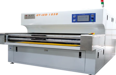
1. Photoresist Application and UV Exposure
A photoresist layer is applied over the copper. Using UV light, the circuit pattern is projected onto the board, hardening the photoresist on trace areas while leaving other parts soft and removable. This transfers the design onto the board.
2. Chemical Etching
The board is then chemically etched to remove unprotected copper, leaving only the desired conductive traces. Careful control prevents over-etching, preserving trace integrity.
3. Cleaning and Inspection
After etching, the photoresist is removed, and the board is cleaned. Visual and automated inspections ensure traces are intact and defect-free, guaranteeing quality in PCB production.
Drilling and Via Plating
Drilling and via plating are essential steps in PCB production, especially for multilayer boards, where precise interlayer electrical connections are required.
1. CNC Drilling
Computer Numerical Control (CNC) machines drill precise holes in the PCB substrate. These holes serve as through-holes for component leads and vias that connect different copper layers electrically. Accuracy in drilling is critical to ensure proper alignment and fit of components, as well as reliable electrical paths.
2. Electroless Copper Plating
After drilling, the holes are coated with a thin layer of copper through an electroless plating process. This conductive layer lines the hole walls, creating a reliable electrical connection between the PCB's internal layers. This step is crucial for multilayer PCBs, where signal integrity and electrical continuity depend on well-formed vias.
3. Importance of Accuracy in Multilayer PCB Production
In complex multilayer boards, even slight misalignments during drilling or plating can cause electrical failures or reduce performance. Therefore, strict quality control and precision equipment are vital during these stages of PCB production to maintain the board's integrity and functionality.
Layer Alignment and Lamination (for Multilayer PCBs)
In the PCB production of multilayer boards, layer alignment and lamination are critical steps that ensure the board's structural strength and electrical functionality.
1. Precise Layer Alignment
Multilayer PCBs consist of multiple inner copper and substrate layers that must be perfectly aligned before lamination. Misalignment can lead to circuit failures or short circuits. Specialized equipment and optical systems are used to accurately position each layer, ensuring that vias and traces match up across the stack.
2. Heat and Pressure Lamination
Once aligned, the layers are bonded together using heat and pressure in a lamination press. This process fuses the layers into a single, solid board, using pre-preg (pre-impregnated bonding sheets) as adhesive material. Proper temperature and pressure settings are essential to avoid delamination or warping.
3. Ensuring Structural Integrity and Electrical Performance
The lamination process not only solidifies the PCB mechanically but also maintains electrical isolation between layers where needed. This step guarantees the finished board can withstand mechanical stresses and perform reliably in complex electronic systems.
Solder Mask and Silkscreen Printing
In the PCB production process, applying the solder mask and silkscreen layers are crucial for protecting the circuitry and aiding in assembly.
1. Applying the Solder Mask
The solder mask is a protective polymer layer applied over the copper traces. Its primary function is to prevent oxidation and avoid solder bridges during component soldering by exposing only the pads where components are mounted. Typically green but available in various colors, the solder mask enhances the PCB's durability and electrical reliability. Precise application ensures that solder flows only where intended, reducing assembly defects.
2. Adding the Silkscreen
After solder mask application, the silkscreen layer is printed on the PCB surface. This layer contains labels, component outlines, logos, and identification marks that help technicians during assembly, testing, and repair. Clear and accurate silkscreen printing improves manufacturing efficiency and reduces errors, ensuring proper component placement.

Surface Finishing
Surface finishing is a critical step in PCB production that enhances solderability and protects the exposed copper surfaces from oxidation and corrosion.
1. Common Surface Finishes
Several finishing techniques are commonly used in the industry, including:
HASL (Hot Air Solder Leveling): A widely used finish where the PCB is dipped in molten solder and then leveled with hot air. It provides good solderability and is cost-effective but may not be ideal for very fine-pitch components.
ENIG (Electroless Nickel Immersion Gold): A popular lead-free finish offering excellent flatness, corrosion resistance, and long shelf life. ENIG is ideal for high-reliability applications and fine-pitch components.
OSP (Organic Solderability Preservative): A thin organic coating that protects copper surfaces and is environmentally friendly. OSP is suitable for simple PCBs and offers excellent solderability but has a shorter shelf life compared to metallic finishes.
2. Purpose of Surface Finishing
The main goals of surface finishing in PCB production are:
Enhancing solderability: Ensuring that solder adheres well to the PCB pads during assembly, improving joint reliability.
Protecting copper: Preventing oxidation and corrosion of the copper traces and pads, which could degrade electrical performance over time.
Improving shelf life: Extending the storage time of PCBs before assembly without compromising quality.
Conclusion
The PCB production process involves multiple precise steps—from design and material selection to etching, drilling, layering, finishing, and testing. Each stage plays a vital role in ensuring the final circuit board meets stringent quality and performance standards.
Precision and rigorous quality control throughout manufacturing are essential to produce reliable PCBs that power today's advanced electronic devices.
For the best results, partnering with experienced and professional PCB production manufacturers is key to achieving high-quality, dependable circuit boards that support innovative technologies.


