Did you know that the precision of circuit boards can make or break a device? In PCB production, exposure plays a critical role in achieving this accuracy. The PCB exposure machine ensures precise circuit patterns by using UV light to activate photoresist.
In this post, we’ll dive into how exposure works in PCB production. You’ll learn about the key processes and how PCB exposure machines help automate and improve efficiency.
What is PCB Exposure?
The Fundamentals of Exposure in PCB Manufacturing
PCB exposure is a critical step in manufacturing printed circuit boards (PCBs). It uses light to transfer circuit designs onto the PCB surface, a process facilitated by a PCB exposure machine. Here's how it works.
Definition of Exposure in PCB Production
During PCB exposure, a photoresist (often dry film) is applied to a copper-clad laminate. The PCB exposure machine then uses ultraviolet (UV) light to harden specific areas of the photoresist. These areas will form the circuit patterns, while the rest remains soluble and can be removed.
UV light plays a central role in this process. It activates the photoresist, triggering a chemical reaction that hardens it. The PCB exposure machine ensures the right amount of UV light is applied for precision and accuracy.
How Exposure Creates Circuit Patterns
The photoresist reacts to UV light in two stages: polymerization and crosslinking. Here's a breakdown:
Polymerization: When the photoresist absorbs UV light, it undergoes a chemical change. This makes the exposed areas solid and resistant to solvents during the development phase.
Crosslinking: This stage links the polymer molecules together, creating a hardened structure that holds the circuit pattern.
In the process, the PCB exposure machine carefully controls the UV light exposure, ensuring the pattern is accurately transferred to the PCB. This results in precise and reliable circuit paths on the final product.
Types of Exposure in PCB Production
Exploring Different Exposure Techniques
Exposure is a crucial step in PCB production. It defines the circuit patterns on the board, and different exposure methods offer unique benefits. Let’s look at three main techniques used in the industry.
Line Exposure
Line exposure is one of the most common methods. During this process, a photosensitive film is applied to the copper-clad PCB. The PCB exposure machine then shines UV light through a negative image of the circuit pattern, which hardens the exposed areas.
How It Works: The areas exposed to UV light become resistant to solvents. The unexposed regions wash away during the development stage.
Applications: This method is widely used in mass production, where high accuracy and speed are essential.
Benefits: It's ideal for large-scale production due to its efficiency and high precision. The PCB exposure machine ensures quick, consistent results.
Solder Resist Exposure
Solder resist exposure is another essential technique. It uses the PCB exposure machine to apply a protective layer over the board, except for the areas that need to be soldered.
How It Works: A photosensitive resist is applied, then exposed to UV light. The pads to be soldered remain unexposed, while the surrounding areas are hardened.
Importance: This process ensures that the solder mask adheres tightly to the PCB surface, protecting the board during the soldering process. It's crucial for the integrity of the pads and the overall quality of the PCB.
Other Exposure Methods
While line and solder resist exposure are standard, there are other methods that provide additional flexibility in certain PCB designs.
Contact Printing: The photomask touches the PCB during exposure. It's cost-effective but can be less precise, especially with fine designs.
Proximity Printing: A small gap between the photomask and PCB helps reduce wear on both. It offers better resolution than contact printing.
Projection Printing: This advanced method uses lenses to project the photomask's image onto the PCB from a distance, achieving high resolution with minimal distortion.
The PCB exposure machine can handle these methods, offering manufacturers the flexibility to choose the best technique based on their needs and the complexity of the design.
How Does Exposure Work in PCB Manufacturing?
Step-by-Step Overview of the Exposure Process
In PCB manufacturing, exposure is a key step to create precise circuit patterns. Here’s a breakdown of how it works:
Preparation Stage: Coating the PCB with Photoresist
Before exposure, the PCB substrate is coated with a light-sensitive material called photoresist. Two main types of photoresist are used:
Photoresist is crucial because it forms the basis of the circuit pattern. It reacts to UV light, which helps define the circuit design.
Placement and Alignment of the Photomask
Next, the photomask is placed over the photoresist layer. The photomask holds the desired circuit pattern, acting as a stencil. Alignment is critical here, as even a small misalignment can result in faulty circuit patterns.
The PCB exposure machine helps ensure the mask is correctly aligned. It uses precision mechanics to position the PCB, ensuring the light passes through only the transparent areas of the photomask.
The Exposure Stage: Application of UV Light
During exposure, the PCB is exposed to UV light. The PCB exposure machine plays a vital role here. It directs UV light onto the photoresist through the photomask. The light activates the photoresist, triggering a chemical reaction that forms the circuit design.
Different light sources are used, including:
These light sources provide the necessary UV intensity to ensure proper exposure.
Development Stage
After exposure, the PCB goes through the development process. The exposed areas of the photoresist harden, while the unexposed parts remain soft. The soft parts are washed away using a developer solution, revealing the circuit pattern.
Proper exposure time and machine calibration are critical. Too much or too little exposure can affect the development stage. The PCB exposure machine helps maintain the correct exposure time for optimal results.
Why Is Exposure Crucial for High-Quality PCB Manufacturing?
The Impact of Proper Exposure on Final PCB Performance
Ensuring Accurate Circuit Patterns
Exposure is essential for transferring precise circuit patterns onto the PCB. During the exposure process, PCB exposure machines use UV light to activate the photoresist, which hardens the exposed areas. This ensures that only the desired patterns remain after development.
When exposure is accurate, it guarantees that the electrical connections align perfectly, preventing faults in the finished circuit board. Without proper exposure, defects can occur, resulting in poor conductivity and potential failures in electronic devices.
High Resolution for Modern Applications
As technology advances, the need for high-resolution PCBs increases. Exposure is crucial for producing intricate, high-density circuit boards, which are now common in smartphones, computers, and other advanced devices.
The precision achieved through exposure ensures that even the smallest features on the PCB are clearly defined, allowing for tight component placements. This high resolution is key to keeping up with the demands of modern electronics.
Layer Alignment in Multi-layer PCBs
In multi-layer PCBs, accurate alignment of the layers is essential for proper functionality. Exposure plays a significant role in aligning vias and interlayer connections, ensuring that all layers fit together seamlessly.
PCB exposure machines contribute to this precision by maintaining tight tolerances throughout the exposure process. Even a small misalignment can result in a faulty connection, so proper exposure is critical to achieving the correct layer alignment and ensuring the overall reliability of the board.
Conclusion
Exposure is a crucial step in PCB production. It ensures precise circuit patterns, which are essential for high-quality PCBs. The right exposure process leads to better performance and reliability in the final product.
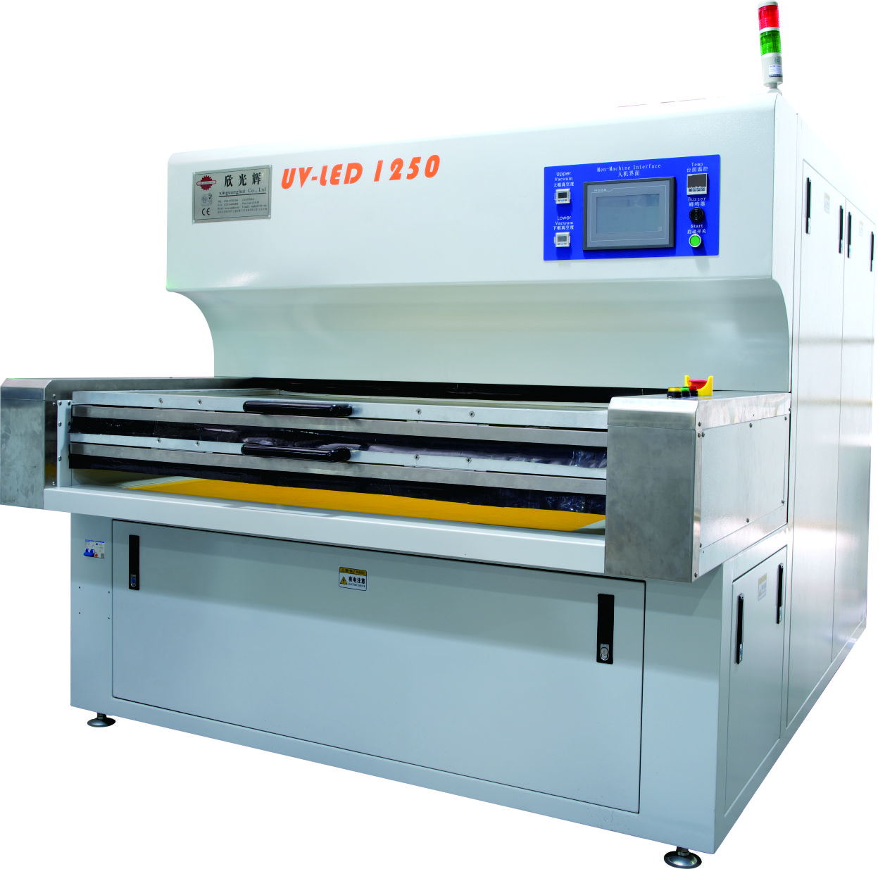
At Shenzhen Xin Guanghui Technology Co., Ltd., we specialize in high-quality machinery for PCB exposure and related processes. Our extensive range includes the Automatic Exposure Machine, Dry Film Laminators, and Manual Exposure Machines. These machines are designed to enhance precision, increase automation, and improve overall production quality in PCB manufacturing.
FAQs
Q: How does UV light affect photoresist during PCB exposure?
A: UV light triggers a chemical reaction in the photoresist, causing it to polymerize. This reaction creates a protective layer that forms the circuit pattern on the PCB after development.
Q: What is the role of a photomask in PCB exposure?
A: The photomask serves as a stencil, blocking UV light in specific areas, allowing only desired sections to be exposed. It ensures accurate circuit pattern transfer onto the PCB.
Q: Can exposure problems be fixed after PCB production?
A: Once exposure problems occur, fixing them is challenging. However, careful inspection and adjustments during production can minimize such issues before the final stages.


