Printed Circuit Boards (PCBs) are the foundation of modern electronics. They provide the structure and pathways that allow electronic components—such as resistors, capacitors, and chips—to work together efficiently. From smartphones and laptops to automotive systems and medical devices, PCBs power the digital world around us.
As devices become smaller and more powerful, the demands on PCB design and manufacturing grow. Today's PCB production requires advanced materials, precise engineering, and strict quality control to meet performance expectations.
Understanding the basics of PCBs—their structure, types, and how they are produced—is essential for anyone involved in electronics, whether you're an engineer, buyer, or simply curious about what makes your devices tick. A deeper look into PCB production reveals how critical it is to modern innovation.
In this article, we'll explore what PCBs are, how they're made, and why high-quality production is vital to the reliability and functionality of electronic products.
What is a PCB?
A Printed Circuit Board (PCB) is a thin, flat board made of insulating material—typically fiberglass or composite epoxy—that mechanically supports and electrically connects various electronic components using conductive pathways etched from copper sheets. These components may include microchips, transistors, resistors, capacitors, and connectors, all arranged in precise locations to carry out specific functions.
1. Definition and Structure
At its core, a PCB serves as the foundation of an electronic system. It provides both mechanical stability to hold components in place and electrical routing to allow current to flow between them. The copper traces act like wires but are integrated into the board in a much more compact and reliable way. Depending on complexity, PCBs may have:
A single layer (simple circuits),
Double layers (used in most everyday electronics),
Or multilayer structures (up to dozens of layers), especially for complex systems like servers or smartphones.
2. Primary Functions
The two primary roles of a PCB are:
Mechanical Support: PCBs securely hold electronic components in fixed positions, maintaining the integrity of the overall circuit even under vibration or movement.
Electrical Connection: Through the use of conductive copper traces and vias (tiny holes that connect different layers), PCBs create defined electrical pathways that allow signals and power to flow precisely where needed.
These dual functions make PCBs not just carriers but active participants in the performance and reliability of electronic devices.
3. Common Applications
PCBs are used across nearly every industry and product involving electronics. Some of the most common applications include:
Consumer Electronics: Smartphones, tablets, televisions, gaming consoles, wearables
Computing Devices: Laptops, desktops, servers, data storage systems
Automotive Electronics: Digital dashboards, engine control units, infotainment systems, ADAS (Advanced Driver Assistance Systems)
Medical Devices: ECG monitors, diagnostic equipment, portable medical tools
Industrial Controls & IoT: PLCs (Programmable Logic Controllers), smart sensors, factory automation systems

Basic Structure of a PCB
Understanding the structure of a PCB is essential to appreciating the precision required in PCB production. Despite varying designs, most PCBs share several key layers that provide mechanical support and reliable electrical connections.
1. Substrate (Base Material)
The substrate is the insulating base of the PCB, offering strength and stability. The most common material is FR4, known for its durability and heat resistance. For specialized needs, materials like ceramic or polyimide are used for better flexibility or thermal performance.
2. Copper Layer
A thin copper layer is applied on the substrate and etched to form conductive traces.
Single-sided PCBs: copper on one side
Double-sided PCBs: copper on both sides with vias
Multilayer PCBs: several copper and substrate layers stacked together
Accurate copper patterning is a critical aspect of PCB production that affects circuit performance.
3. Solder Mask
The solder mask is a protective coating over copper traces that prevents oxidation and solder bridging. Usually green, it also enhances appearance and aids in assembly. Its quality directly impacts board reliability and ease of manufacturing.
4. Silkscreen
Printed on top of the solder mask, the silkscreen provides component labels, logos, and guides for assembly. Clear markings help reduce errors during testing and repairs.
5. PCB Type Comparison
Single-sided: Basic, low-cost, used in simple electronics
Double-sided: Copper and components on both sides; moderate complexity
Multilayer: High-density circuits for advanced devices like smartphones and automotive systems
Types of PCBs
In PCB production, understanding the different types of printed circuit boards helps engineers and manufacturers choose the right solution for each application. PCBs vary in structure and material to meet different functional and environmental needs.
1. Single-Sided PCBs
These are the most basic PCBs, with copper traces on only one side of the substrate. Components are mounted on the same side as the copper layer.
Applications: Calculators, power adapters, basic home appliances
Advantages: Low cost, simple design, easy to produce
Limitations: Limited functionality, not suitable for complex circuits
Production: Involves fewer steps, making it cost-effective
2. Double-Sided PCBs
These boards have copper layers on both sides, connected by plated vias, allowing more complex routing.
Applications: Industrial controls, audio systems, consumer electronics
Advantages: Greater circuit density, better performance
Production Considerations: Requires accurate drilling and plating for reliable interlayer connections
3. Multilayer PCBs
With three or more copper layers laminated together, these PCBs support complex designs in a compact form.
Applications: Smartphones, laptops, automotive electronics, medical devices
Advantages: High density, good signal integrity, space-saving
Challenges: More complex PCB production, needing precise layer alignment and advanced testing
4. Rigid, Flexible, and Rigid-Flex PCBs
PCBs can also be categorized by their physical structure:
Rigid PCBs: Solid and inflexible, widely used
Flexible PCBs: Bendable, ideal for foldable or wearable devices
Rigid-Flex PCBs: Combine both types, suited for compact, high-performance systems in aerospace and medical tech
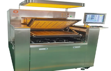
PCB Production Process Overview
The PCB production process turns a design into a working circuit board through several key steps:
1.Design Stage
Using software like Altium Designer or KiCAD, engineers create detailed PCB layouts that guide manufacturing.
2.Material Preparation & Image Transfer
The PCB pattern is transferred onto copper-coated substrate via photo plotting or dry film.
3.Etching & Cleaning
Unwanted copper is removed, leaving conductive traces; the board is then cleaned.
4.Drilling & Plating
Holes and vias are drilled and plated to connect layers electrically.
5.Solder Mask, Silkscreen & Surface Finishing
Protective solder mask and labeling silkscreen are applied; surface finishes improve solderability.
6.Testing & Assembly
Electrical and functional tests ensure quality before components are mounted.
Why PCB Production Matters
1. Ensuring Performance and Reliability
High-quality PCB production directly affects the performance, durability, and safety of electronic devices. A well-manufactured PCB minimizes signal loss, prevents short circuits, and ensures stable operation—even in harsh environments. Poor production, on the other hand, can lead to failures, product recalls, or even safety hazards.
2. Enabling Advanced Technologies
Precision in PCB production is essential for supporting modern innovations. Technologies such as autonomous driving, 5G communication, and AI-powered devices rely on complex multilayer PCBs with high-speed signal integrity and low interference. These advanced applications demand ultra-reliable boards produced with tight tolerances and rigorous quality control.
3. Supporting Product Innovation and Scalability
Efficient PCB manufacturing not only supports current technologies but also enables faster prototyping and scalable mass production. This accelerates time-to-market and helps businesses stay competitive in fast-evolving industries.
Conclusion
Printed Circuit Boards (PCBs) are the foundation of all modern electronics, serving both as mechanical support and as critical electrical connectors. From simple single-sided boards to complex multilayer and flexible designs, each type serves specific needs across various industries.
Understanding the structure, types, and PCB production process helps highlight just how essential quality manufacturing is. Reliable PCB production ensures not only device performance and safety but also supports the demands of emerging technologies like 5G, AI, and autonomous systems.
As the electronics industry continues to evolve, staying informed about PCB innovations is more important than ever. For businesses seeking long-term success, partnering with experienced and professional PCB production providers is a smart step toward achieving high-quality, future-ready products.


