The world of modern electronics depends heavily on Printed Circuit Boards (PCBs). These boards serve as the backbone of nearly every device we use daily, from mobile phones and computers to cars, medical equipment, and aerospace systems. Without PCBs, it would be impossible to achieve the compact size, high performance, and reliability that today’s devices demand.
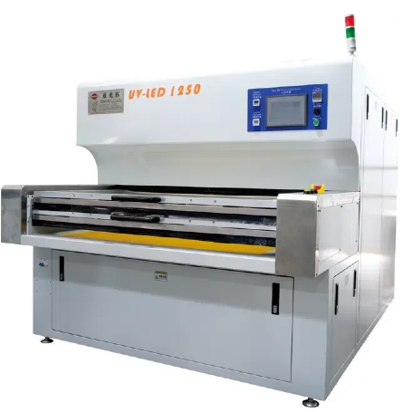
Among the many steps involved in PCB manufacturing, one of the most important is circuit imaging, the process of transferring the circuit design onto the board. At the heart of this step lies the PCB exposure machine, a specialized piece of equipment designed to expose photoresist-coated boards to light in order to create the exact patterns of the desired circuits.
This article will provide a detailed explanation of why PCB exposure machines are essential in circuit fabrication, how they work, the different types available, and the key factors that influence their selection and performance. By the end, you will understand how exposure machines contribute to the precision and reliability of modern electronic products.
What is a PCB Exposure Machine?
A PCB exposure machine is equipment used during the photo-lithography process in PCB production. After a copper-clad board has been laminated with a layer of photosensitive dry film resist, the exposure machine shines light through a mask or film that contains the circuit pattern. The light hardens specific areas of the film while leaving other areas unexposed, which can later be developed and etched to form the copper traces of the circuit.
In simple terms, the exposure machine acts like a printer—but instead of ink, it uses light to “print” a pattern onto the photoresist. The accuracy of this exposure determines how well the final circuit matches the intended design.
Why Exposure Machines are Crucial in PCB Fabrication
The exposure step is one of the most delicate parts of PCB manufacturing. A small error here can lead to circuit defects, reduced yield, or even complete product failure. Some of the main reasons PCB exposure machines are so important include:
High Precision in Pattern Transfer
Exposure machines ensure that even the finest details of a circuit design are transferred accurately onto the board. This is vital for today’s miniaturized electronics, where line widths and spacing can be measured in micrometers.
Consistency Across Production
In mass production, consistency is key. Exposure machines provide uniform light intensity and precise alignment, ensuring that every board in a batch has the same quality.
Support for Fine-Line Circuits
As devices become smaller, circuits must also shrink. Exposure machines allow manufacturers to achieve ultra-fine patterns that manual or outdated methods could never produce.
Reduced Defects and Higher Yield
Precise exposure minimizes defects such as misalignment, underexposure, or overexposure. This increases the number of usable boards and lowers overall production costs.
Compatibility with Advanced PCB Types
Multilayer PCBs, HDI (High-Density Interconnect) boards, and flexible PCBs all require precise exposure to function properly. Without modern exposure technology, producing these advanced boards would be nearly impossible.
")
How a PCB Exposure Machine Works
Although different models of exposure machines may vary in complexity, the basic working principle remains the same. The process can be broken down into several steps:
1. Preparation of the Board
The copper-clad board is first coated with a layer of photoresist, typically a dry film that is sensitive to ultraviolet (UV) light.
2. Mask Alignment
A photomask (a transparent film with opaque circuit patterns) is carefully aligned over the board. This alignment is critical because even the slightest misplacement can cause circuit errors.
3. Light Exposure
The machine projects UV light through the mask. The transparent areas of the mask allow light to harden the photoresist, while the opaque areas block it, leaving those regions unexposed.
4. Development
After exposure, the board is developed in a chemical solution that washes away the unexposed photoresist. The hardened areas remain intact, protecting the copper beneath them.
5. Etching
The board is then placed in an etching solution that removes the unprotected copper. What remains is the precise copper circuit pattern that matches the design.
This process highlights why exposure machines are so essential: if the exposure step is not accurate, the resulting board will have misaligned or defective circuits.
Types of PCB Exposure Machines
Different types of exposure machines are used depending on the complexity of the PCB and the production scale.
1. Contact Exposure Machines
These machines press the mask directly against the photoresist-coated board during exposure. They are relatively simple and cost-effective but can suffer from mask wear and alignment issues over time.
2. Proximity Exposure Machines
In this method, the mask is placed very close to the board without direct contact. This reduces wear and contamination but may slightly reduce resolution compared to contact exposure.
3. Projection Exposure Machines
These use lenses to project the mask image onto the board. This method allows for extremely high precision and is ideal for fine-line circuits, though it is more complex and expensive.
4. Laser Direct Imaging (LDI) Systems
The most advanced type, LDI systems eliminate the need for a physical mask. Instead, they use computer-controlled lasers to directly “draw” the circuit pattern onto the photoresist. This provides unmatched accuracy and flexibility, especially for HDI and multilayer boards.
Key Factors Affecting Exposure Quality
Several variables influence how well a PCB exposure machine performs:
Light Intensity and Uniformity: Consistent light across the entire board ensures even exposure and prevents weak spots.
Wavelength of Light: UV light is typically used, but the exact wavelength must match the sensitivity of the photoresist.
Mask Quality: Any defect in the mask will be transferred to the board. High-quality masks or digital imaging systems are essential.
Alignment Systems: Automated alignment systems improve precision and reduce human error, especially for multilayer PCBs.
Environmental Control: Exposure rooms must be clean and dust-free, as particles can cause defects during the process.
Industry Applications of PCB Exposure Machines
Exposure machines are vital across industries that demand reliable and complex electronics:
Consumer Electronics – Smartphones, tablets, and wearables rely on miniaturized PCBs with fine circuits.
Automotive Electronics – Safety systems, sensors, and electric vehicle control units depend on durable, high-quality boards.
Medical Devices – Life-critical equipment requires error-free PCBs manufactured under strict standards.
Telecommunications – Routers, servers, and network devices need precise boards to handle high-speed signals.
Aerospace and Defense – Exposure machines support boards that must perform in extreme conditions with zero tolerance for defects.
Challenges in PCB Exposure
Even with advanced machines, exposure remains a challenging step. Some common issues include:
Misalignment – Slight shifts in mask alignment can cause circuit errors.
Overexposure or Underexposure – Incorrect light levels can either harden too much of the resist or leave parts too soft.
Dust and Contamination – Particles trapped between the mask and board create defects.
Material Sensitivity – Different photoresists require different exposure parameters, adding complexity to the process.
Manufacturers must combine high-quality machines with strict process controls to overcome these challenges.
The Future of PCB Exposure Machines
As technology advances, exposure machines are evolving to meet new demands. Some of the trends shaping the future include:
Laser Direct Imaging Expansion – LDI is becoming more common as the demand for fine-line and high-density circuits increases.
Automation and AI Integration – Smart machines that can self-correct exposure parameters and detect defects in real time are emerging.
Eco-Friendly Processes – New machines are being designed to reduce energy consumption and minimize chemical use.
Support for Flexible and Rigid-Flex Boards – With the growth of wearable devices, machines capable of handling flexible substrates are becoming essential.
These innovations will ensure that exposure machines remain at the heart of PCB manufacturing for decades to come.
Conclusion
The importance of PCB exposure machines in circuit fabrication cannot be overstated. They serve as the link between design and reality, transferring intricate patterns onto copper boards with precision and consistency. Whether in consumer electronics, automotive systems, medical devices, or aerospace technology, the exposure process determines the success of the entire product.
By offering high accuracy, repeatability, and support for advanced designs, PCB exposure machines enable manufacturers to meet the demands of modern electronics. As technology continues to evolve, these machines will only become more advanced, ensuring that PCBs remain the reliable foundation of our digital world.


