Printed Circuit Board (PCB) fabrication is a cornerstone of modern electronics, forming the backbone of everything from consumer devices to industrial machinery. A key process in PCB manufacturing is the exposure of the photoresist layer, which is crucial for transferring circuit patterns onto the board. In this context, the CCD Line Exposure Machine has become an indispensable tool for ensuring high-precision and high-quality PCBs.
CCD (Charge-Coupled Device) technology has revolutionized the PCB fabrication process. It is widely used in applications such as photoresist exposure for the transfer of circuit patterns, particularly in the manufacturing of multilayer and high-density PCBs. The machine works by exposing a layer of photoresist on the PCB to light, where the patterns of the PCB circuit are imaged onto the resist. The precision of this process is crucial, and the CCD Line Exposure Machine delivers the accuracy and performance required for today’s increasingly complex and intricate PCB designs.
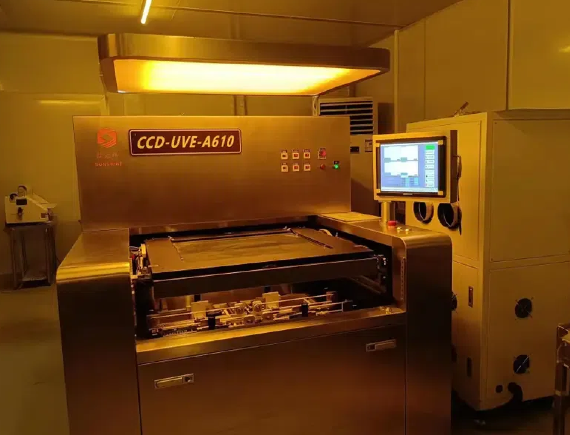
What is a CCD Line Exposure Machine?
The CCD Line Exposure Machine is an advanced tool designed to expose the photoresist layer of PCBs during the imaging process. Using a high-resolution CCD camera or sensor, the machine captures the image of the circuit pattern and projects it onto the board with high precision. The line exposure process is commonly used for PCB manufacturing, particularly for smaller boards or those requiring high accuracy. In some configurations, it can expose multiple boards at once, making it highly efficient.
A key feature of these machines is their ability to deliver high accuracy, with a contrast mechanical accuracy of ±15μm, which is critical when working with intricate circuit designs. The machine’s CCD camera, which is sensitive to light, ensures that the exposure process is precise, reducing the risk of alignment errors and ensuring the PCB pattern is faithfully replicated onto the photoresist.
Key Advantages of CCD Line Exposure Machines in PCB Fabrication
1. High Precision and Accuracy
One of the most significant advantages of using CCD Line Exposure Machines is the level of precision they offer. The CCD camera is highly sensitive and can detect the smallest variations in the PCB design. With a contrast mechanical accuracy of ±15μm, these machines can accurately expose even the most intricate circuit patterns, including those with fine traces and small components.
This high level of precision is essential in modern PCB fabrication, where designs are becoming increasingly complex and miniaturized. Whether for consumer electronics, telecommunications equipment, or medical devices, the ability to produce accurate and reliable PCBs is critical. Any slight misalignment in the exposure process can lead to defects in the final product, which could impact the performance and functionality of the electronic device.
2. Faster Production and Higher Throughput
Traditional exposure methods often require multiple manual steps, leading to slower production times and increased chances of human error. CCD Line Exposure Machines, however, are automated and capable of handling multiple boards at once, which greatly speeds up the process. This automation reduces labor costs and minimizes the risk of inconsistencies in the exposure process.
Moreover, these machines allow for higher throughput, meaning more boards can be produced in a shorter time frame. This is particularly advantageous for high-volume PCB manufacturers who need to meet tight deadlines or keep up with high demand in industries such as automotive, telecommunications, and consumer electronics.
By improving production speed and throughput, CCD Line Exposure Machines enable manufacturers to reduce their overall costs, improve efficiency, and stay competitive in a rapidly evolving market.
3. Superior Image Quality
The quality of the image produced by the CCD sensor plays a crucial role in ensuring that the circuit patterns are correctly transferred onto the PCB. Unlike traditional exposure systems, which may suffer from image distortion or blur, the CCD Line Exposure Machine produces crisp, sharp images that accurately represent the design.
The high-resolution capabilities of the CCD camera ensure that even the smallest details of the circuit are captured and projected with precision. This superior image quality is especially important when manufacturing complex multilayer PCBs, where even slight imperfections can result in poor performance, electrical failure, or short circuits.
Additionally, CCD sensors can adjust the exposure based on the thickness and type of the photoresist, ensuring optimal results in a wide variety of manufacturing conditions. This makes the CCD Line Exposure Machine adaptable and capable of handling different types of PCBs, from simple to highly complex designs.
4. Improved Alignment and Reduced Errors
PCB fabrication often involves multiple layers that must be aligned with great precision to ensure the final board works as intended. The alignment process can be challenging, especially when working with double-sided or multilayer boards. CCD Line Exposure Machines are designed to address these challenges by using advanced automatic alignment systems.
The CCD sensor is capable of detecting even the smallest misalignments between the layers or the circuit pattern and adjusting the exposure accordingly. This reduces the chances of exposure errors, such as misalignment or image distortion, which can lead to defective boards. By improving alignment accuracy, CCD machines ensure that each layer of the PCB is properly imaged, contributing to the overall reliability and functionality of the finished product.
5. Cost-Effective and Efficient
Although the initial cost of a CCD Line Exposure Machine may be higher than traditional exposure systems, the long-term benefits far outweigh the investment. The automation and precision of these machines lead to fewer defects, reduced material waste, and shorter production times. As a result, manufacturers can save on costs related to rework, scrap, and labor.
By improving efficiency and minimizing the risk of errors, CCD Line Exposure Machines help PCB manufacturers maximize their output while reducing operational costs. For high-volume PCB producers, this cost-effectiveness is essential for maintaining profitability and staying competitive in the market.
Additionally, the low maintenance requirements of CCD Line Exposure Machines contribute to their cost-effectiveness. These machines are designed for long-term reliability, with durable components that require minimal upkeep, reducing downtime and maintenance costs.
6. Reduced Waste and Environmental Impact
Environmental sustainability is becoming an increasingly important consideration in PCB fabrication. Traditional exposure methods can lead to significant material waste, including photoresist and chemicals. However, CCD Line Exposure Machines reduce material waste by ensuring that the exposure is as accurate as possible.
Because the exposure process is more precise, there is less need for excess photoresist material, leading to a reduction in chemical waste. This not only helps PCB manufacturers reduce their environmental impact but also lowers the costs associated with purchasing and disposing of materials. Furthermore, the precision of the exposure process minimizes the chances of defective boards, further reducing the need for rework and scrap.
7. Adaptability to Various PCB Designs
The versatility of the CCD Line Exposure Machine allows it to handle a wide range of PCB designs, from simple single-layer boards to complex multilayer and HDI (high-density interconnect) designs. The high-resolution imaging capabilities and automatic alignment make these machines ideal for handling different types of photoresists, substrates, and circuit patterns.
As the demand for more sophisticated PCBs increases, manufacturers need equipment that can adapt to new design requirements. The CCD Line Exposure Machine meets this need by offering flexibility and precision across a broad spectrum of PCB designs.
8. Support for Advanced Technologies
The PCB industry is constantly evolving, with new technologies such as 5G, IoT, and automotive electronics pushing the boundaries of PCB design. As a result, manufacturers need exposure systems that can handle the growing complexity of these designs. CCD Line Exposure Machines are equipped to support these advancements by providing the precision, speed, and reliability required for next-generation PCBs.
Additionally, these machines are often compatible with other advanced PCB manufacturing technologies, such as laser direct imaging (LDI) or automated optical inspection (AOI), further enhancing their capabilities. The integration of these technologies ensures that the entire PCB manufacturing process remains streamlined and efficient.
Conclusion
The CCD Line Exposure Machine has become a cornerstone in modern PCB fabrication due to its precision, speed, cost-effectiveness, and adaptability. Its ability to provide high-resolution exposure with contrast mechanical accuracy of ±15μm ensures that manufacturers can produce high-quality, reliable PCBs for a wide range of applications. With its advantages in precision, efficiency, image quality, and reduced waste, the CCD Line Exposure Machine is an essential tool for PCB manufacturers who want to stay ahead in an increasingly competitive market.
As PCB designs become more complex and the demand for advanced electronics grows, investing in CCD Line Exposure Machines offers a clear path forward for manufacturers looking to improve their production processes, reduce costs, and meet the demands of the future. With these machines, the future of PCB fabrication looks brighter, more efficient, and more sustainable than ever before.


