In today’s electronics-driven world, Printed Circuit Boards (PCBs) form the foundation of nearly every modern device. From smartphones and laptops to medical devices, automobiles, and aerospace equipment, PCBs make it possible to integrate complex circuits into compact, reliable, and efficient designs. As the demand for higher performance and smaller, more sophisticated electronics grows, the requirements for PCB quality and production efficiency become more demanding than ever.
One technology at the heart of this transformation is the PCB exposure system. These machines play a crucial role in transferring precise circuit patterns onto boards during the manufacturing process. By harnessing advanced exposure systems, manufacturers can significantly boost productivity, improve product quality, and reduce costs—all while keeping up with the ever-evolving standards of the electronics industry.
This article explores how advanced PCB exposure systems enhance both productivity and quality, the technologies driving their performance, the challenges they help overcome, and the impact they have across industries.
Understanding PCB Exposure Systems
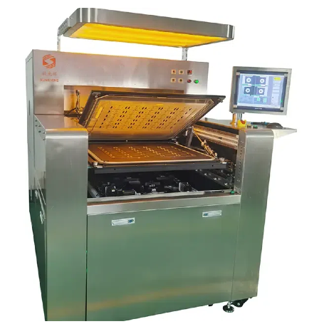
PCB exposure systems are specialized machines used in the photolithography stage of PCB fabrication. After a copper-clad board is coated with a photosensitive resist, the exposure system projects light through a patterned mask or directly onto the board to define the circuit design. The exposed areas of the resist harden, while the unexposed areas can later be developed and etched away, leaving behind the copper traces that form the circuits.
In essence, the exposure system functions like a high-precision printer—but instead of ink, it uses light to transfer patterns with microscopic accuracy. The performance of this step directly determines the accuracy, consistency, and reliability of the final board.
Why Advanced Exposure Systems Matter
The shift from traditional electronics to miniaturized, high-density, and high-performance devices has pushed PCB manufacturers to embrace more sophisticated exposure technologies. Here’s why advanced systems are so important:
Higher Precision for Fine-Line Circuits
Today’s devices often require circuits with line widths and spacing as small as a few micrometers. Advanced exposure systems provide the precision necessary to achieve these fine features without defects.
Improved Productivity in Mass Production
Modern systems offer faster processing speeds, enabling manufacturers to handle high volumes without sacrificing quality. This is especially critical for industries like consumer electronics, where demand is high and time-to-market is short.
Consistency Across Boards
Advanced machines ensure uniform exposure across every board, minimizing variations that could compromise performance. Consistency is essential when producing thousands or millions of units.
Support for Complex PCB Designs
With the rise of multilayer PCBs, HDI (High-Density Interconnect) boards, and flexible circuits, exposure systems must be capable of handling intricate patterns and precise alignments.
Reduced Defects and Rework
By using advanced optics, automation, and digital imaging, these systems reduce errors caused by misalignment, underexposure, or contamination, thereby lowering costs associated with rework or scrap.
How Advanced PCB Exposure Systems Work
The core process of a PCB exposure system has remained the same for decades, but technology has advanced to increase both accuracy and efficiency. Modern systems typically operate through the following steps:
Preparation – A copper-clad board is laminated with a photoresist layer.
Masking or Imaging – The system either aligns a photomask with the board or uses direct imaging to project the circuit design.
Light Exposure – Ultraviolet (UV) light or laser beams are used to harden specific areas of the resist.
Development – The unexposed resist is washed away, leaving the hardened resist to protect copper traces.
Etching – The unprotected copper is removed, forming the circuit.
What sets advanced exposure systems apart is their use of cutting-edge optics, laser direct imaging (LDI), computer-controlled alignment, and automation. These features allow for unmatched precision and speed, enabling manufacturers to meet the challenges of next-generation electronics.
")
Key Technologies Driving Advanced Exposure Systems
Modern PCB exposure systems integrate a range of innovative technologies that directly boost productivity and quality.
1. Laser Direct Imaging (LDI)
LDI eliminates the need for physical photomasks. Instead, lasers controlled by digital files “draw” the circuit pattern directly on the resist. This reduces preparation time, eliminates mask defects, and provides incredible flexibility for design changes.
2. Automated Alignment Systems
Advanced machines use cameras and software to align layers with sub-micron accuracy. This is especially critical for multilayer boards, where even the smallest misalignment can lead to failure.
3. High-Intensity and Uniform UV Sources
Modern UV lamps or LEDs provide consistent exposure across the entire board, ensuring reliable results even for large panels.
4. AI and Process Control Integration
Some systems now incorporate AI-driven algorithms to automatically adjust exposure parameters in real time, optimizing quality while reducing operator intervention.
5. Eco-Friendly Designs
Energy-efficient lighting systems and reduced chemical usage make advanced exposure machines more sustainable, addressing growing environmental concerns in manufacturing.
Boosting Productivity with Advanced Exposure Systems
One of the most significant advantages of advanced PCB exposure systems is their ability to accelerate production without compromising quality.
Faster Setup Times – With digital imaging and automated alignment, machines can quickly transition between jobs, reducing downtime.
High Throughput – Advanced systems process multiple panels at once or operate at higher speeds, dramatically increasing output.
Reduced Scrap Rates – By minimizing exposure errors, manufacturers save time and resources that would otherwise go into rework.
Scalability – Whether for small prototyping runs or mass production, advanced exposure systems adapt easily to different scales of manufacturing.
For manufacturers facing tight deadlines and growing demand, these productivity gains make a significant difference.
Enhancing Quality with Advanced Exposure Systems
Alongside productivity, quality assurance is equally important in PCB manufacturing. Advanced exposure systems help ensure boards meet the strictest standards.
Micron-Level Accuracy – Critical for fine-line circuits and HDI boards.
Uniform Exposure – Prevents weak spots that could cause open circuits or poor conductivity.
Error Detection – Integrated inspection tools identify misalignments or defects before they impact the final product.
Long-Term Reliability – High-quality exposure ensures that boards perform consistently over time, which is essential in industries like medical and aerospace.
By combining precision with consistency, advanced systems guarantee that every PCB meets performance requirements.
Applications Across Industries
The benefits of advanced PCB exposure systems extend across multiple industries:
Consumer Electronics – Smartphones, tablets, and wearables rely on ultra-fine PCBs produced with high throughput.
Automotive – Safety systems, sensors, and electric vehicle components require highly reliable boards.
Telecommunications – Routers, 5G equipment, and servers demand boards capable of handling high-speed signals.
Medical Devices – Life-critical equipment needs boards manufactured to exacting standards with zero tolerance for defects.
Aerospace and Defense – Exposure systems ensure PCBs can withstand extreme environments without failure.
Each of these sectors benefits directly from the enhanced productivity and quality delivered by advanced systems.
Overcoming Challenges in PCB Exposure
Even with advanced systems, challenges remain in exposure processes. These include:
Handling Smaller Line Widths – As designs shrink, exposure accuracy becomes more critical.
Managing Multilayer Complexity – Aligning multiple layers requires extreme precision.
Environmental Factors – Dust, vibration, or temperature fluctuations can affect exposure quality.
Cost of Investment – Advanced exposure systems require significant upfront costs, though the long-term benefits often outweigh them.
Manufacturers must balance these challenges with the advantages, ensuring proper training, cleanroom environments, and maintenance practices.
The Future of PCB Exposure Systems
Looking ahead, exposure systems will continue to evolve alongside electronics technology. Some trends include:
More Widespread Adoption of LDI – Especially for HDI and flexible PCBs.
Increased Automation – Reducing human error and labor requirements.
Integration with Smart Manufacturing – Linking machines with IoT systems for real-time monitoring and optimization.
Sustainability Focus – Energy-efficient systems and reduced waste will become industry standards.
These innovations will further enhance both productivity and quality, ensuring manufacturers remain competitive in a rapidly advancing market.
Conclusion
In the highly competitive world of electronics manufacturing, advanced PCB exposure systems are no longer optional—they are essential. By combining speed, precision, consistency, and flexibility, these systems enable manufacturers to produce PCBs that meet the demanding requirements of today’s devices while keeping production efficient and cost-effective.
From consumer gadgets to aerospace technology, advanced exposure systems serve as the bridge between design and reality, ensuring that every board delivers both performance and reliability. As the industry continues to evolve, these machines will remain central to driving innovation and meeting the growing demands of modern electronics.
For companies seeking reliable solutions to boost their PCB manufacturing capabilities, Shenzhen Xinhui Technology Co., LTD. stands out as a trusted partner, offering advanced exposure systems designed to enhance both productivity and quality.


