
Are you curious about how circuit patterns are transferred onto PCBs? Dry film lamination plays a crucial role in this process. In PCB manufacturing, dry film lamination applies a photosensitive material to the copper surface. This method offers greater precision and efficiency compared to traditional techniques. In this post, you'll learn about the step-by-step process of dry film lamination and why it's preferred in modern electronics.
What is Dry Film Lamination?
Definition of Dry Film Lamination
Dry film lamination is a process where a photosensitive material, known as dry film, is applied to a substrate, like copper, in PCB production. This material is used to create the intricate circuit patterns that define the electronic components on a board.
A dry film laminator is the key equipment in this process. It ensures that the dry film adheres evenly to the PCB surface by applying heat, pressure, and sometimes vacuum. The laminator's precision helps create high-resolution images essential for modern electronics.
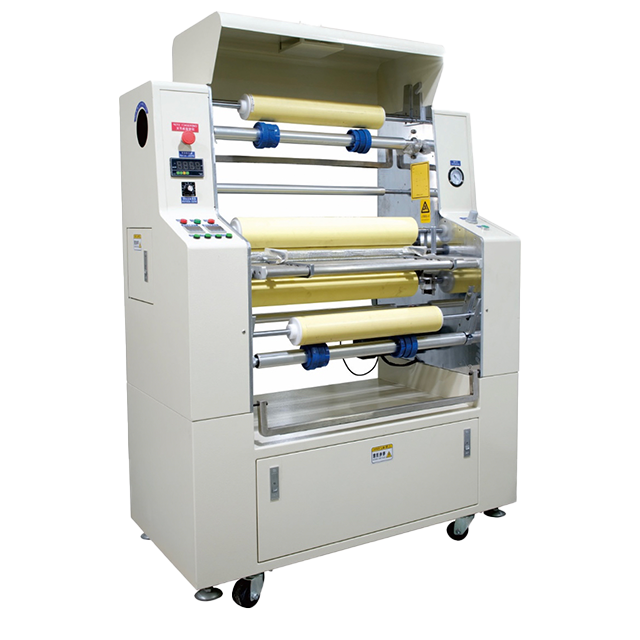
Overview of Dry Film Laminator in PCB Manufacturing
Dry film laminators are crucial in PCB manufacturing. They apply dry film to copper-clad PCBs, ensuring the film bonds securely without air pockets or wrinkles. The laminator's controlled pressure and temperature settings allow the photopolymer layer to adhere evenly, ensuring high-quality results.
This process is essential for creating fine circuit patterns, which are important for advanced, high-performance PCBs used in consumer electronics, automotive devices, and medical equipment.
Key Components of the Dry Film Lamination Process
Dry film lamination involves several critical components that contribute to its efficiency and precision in PCB manufacturing. These components work together to ensure that the circuit design is accurately transferred onto the PCB.
Types of Dry Film Materials
The dry film material used in lamination typically consists of three main layers:
Cover Sheet
The cover sheet is a thin polyester layer that protects the photopolymer during storage and handling. It is removed before the lamination process begins.
Photopolymer Layer
This is the key layer of the dry film, containing a photosensitive material that reacts to UV light. It is responsible for creating the circuit pattern after exposure and development. The photopolymer layer is crucial for achieving high-resolution patterns, enabling fine line widths down to 30 microns.
Support Layer
The support layer is a thicker polyester sheet that provides stability to the photopolymer during the lamination process. It is removed after lamination, leaving the photopolymer adhered to the copper surface of the PCB.
Each layer serves a distinct function to ensure the film adheres properly, resists unwanted etching, and delivers the required resolution in PCB manufacturing.
Equipment Used for Dry Film Lamination
The equipment involved in dry film lamination is equally important for ensuring the film is applied correctly and efficiently. A key piece of equipment is the dry film laminator, which uses precise control of temperature, pressure, and speed to apply the film uniformly.
Dry Film Laminator
The laminator is responsible for bonding the dry film to the copper surface. It uses a combination of heat, pressure, and vacuum to ensure uniform adhesion without air bubbles or wrinkles. The laminator typically heats the dry film to a temperature between 60°C and 80°C before applying it to the PCB.
Adjustable Settings
A good laminator allows operators to adjust temperature, pressure, and speed to suit different types of substrates and film thicknesses. This flexibility ensures that the dry film is applied consistently and with high precision.
Hot Roll Laminator
Hot roll laminators play a key role in achieving the precise bonding of the dry film to the PCB. These machines use heated rollers to apply pressure to the dry film, ensuring that it conforms tightly to the copper surface without forming bubbles or wrinkles. The use of high-quality rollers is critical to maintaining uniform pressure across the entire PCB.
By controlling these parameters, dry film laminators ensure the highest quality in the lamination process, leading to precise and reliable results.
Step-by-Step Process of Dry Film Lamination
Step 1 - Preparing the PCB and Dry Film
The first step is to cut the dry film sheet to match the size of the PCB. This helps minimize waste and ensures the material fits perfectly onto the surface. Be sure the copper surface of the PCB is clean and free from dust, oils, or any other contaminants. A clean surface is crucial for a strong bond between the dry film and the copper.
Step 2 - Removing the Cover Sheet
Now, carefully peel off the thin cover sheet of the dry film. This will expose the photopolymer layer, which will eventually form the resist image. Be gentle when peeling it off—avoiding any damage to the photopolymer layer is key. Try not to stretch the film or cause any tears.
Step 3 - Laminating the Dry Film onto the PCB
Place the PCB and dry film into the laminator. The dry film laminator applies uniform pressure and heat to bond the film to the PCB. The ideal temperature is typically between 60°C to 80°C. The pressure should be high enough to avoid air bubbles or gaps, but not so much that it distorts the film. A vacuum assists in eliminating any air between the dry film and the PCB surface, ensuring an even bond.
Step 4 - Cooling and Removing the Support Layer
Once laminated, let the PCB cool to room temperature. This solidifies the bond between the film and the copper surface. After cooling, carefully peel off the thick support layer. The photopolymer layer will stay firmly attached to the PCB. Use a sharp blade to trim any excess dry film around the edges for a clean finish.
Common Issues in Dry Film Lamination and Solutions
Dry film lamination is a critical step in PCB manufacturing, but it can present some challenges. Let's explore common issues and how to fix them.
Issue 1: Bubbles Between Dry Film and Copper
Bubbles can appear during lamination if pressure is uneven or if the PCB surface is contaminated. These bubbles can affect the quality of the circuit pattern.
Solution:
Ensure uniform pressure by adjusting the laminator's settings.
Clean the PCB surface thoroughly before lamination to remove any dust, grease, or oxidation.
Issue 2: Insufficient Adhesion of Dry Film
Sometimes, the dry film doesn't stick well to the copper, causing adhesion issues. This can happen due to improper pressure or an unclean PCB surface.
Solution:
Increase pressure during lamination to ensure a stronger bond.
Maintain a controlled humidity level in the production environment.
Double-check that the copper surface is free of contamination.
Issue 3: Wrinkling of Dry Film
Wrinkles often form when the PCB is not handled carefully or when excessive pressure is applied. These wrinkles can disrupt the fine details of the circuit design.
Solution:
Adjust laminator pressure and speed settings to prevent excessive force on the dry film.
Lower the temperature if wrinkles persist during lamination.
Handle the PCB gently and ensure even pressure across the surface.
Issue 4: Residual Adhesive on the PCB
Sometimes, adhesive residue remains on the PCB after the dry film is removed. This can interfere with the next steps in PCB manufacturing.
Solution:
By tackling these common issues, you can improve the quality and consistency of your dry film lamination process.
Conclusion
Dry film lamination is a vital process in PCB manufacturing, ensuring high precision and uniformity. The dry film laminator plays a crucial role in achieving flawless adhesion and coverage.
This method is essential for producing high-quality PCBs used in modern electronics. It enables the creation of intricate designs with high resolution.
Explore our Dry Film Laminators for unmatched reliability in your PCB production. Visit Shenzhen Xinhui Technology Co., LTD for more details.
Frequently Asked Questions (FAQs)
1. What is dry film lamination used for in PCB manufacturing?
Dry film lamination is used to apply a photosensitive material onto a PCB, helping to transfer intricate circuit designs onto the copper surface.
2. How does a dry film laminator work?
A dry film laminator uses heat, pressure, and vacuum to bond a thin layer of photoresist film to the copper surface of a PCB, ensuring uniform adhesion.
3. What are the main benefits of using dry film lamination over traditional methods?
Dry film lamination offers higher precision, faster processing, reduced chemical usage, and better environmental friendliness compared to traditional liquid photoresists.


